Thoughts on Sensor Design
I’m launching a summer of environmental sensor work, and I want to make sure I’m not reinventing a wheel. Given that I don’t have any close collaborators at this point who are deep into sensor design and development, I’m asking the cloud for feedback and critique.
The Things We’re Sensing: Temperature, Depth
The fundamental sensing questions involve water: temperature, salinity, and depth.
There’s multiple locations that we might want to investigate, and we might have different sensing desires at different locations; for example, in Casco Bay, we might not want salinity, but we absolutely need depth and temperature, while in the salt marshes of the Morse Mountain Conservation Area, we need salinity, because we’re tracking the influx of tides.
Our Budget Target: $20-40
We’re also sensitive to cost: we’d like to have more, rather than fewer, sensors. This means that $50 enclosures are not OK. A $5 enclosure, if possible, would be lovely. Commercial-off-the-shelf salinity and temperature sensors can run anywhere from $1000 - $2500, but they’re not reusable… so, strictly speaking, our budget targets are rediculously high. But, if we want to have broad sensor coverage, or engage in community-engaged environmental sensing projects, we need to get down into the tens-not-hundreds-of-dollars range for our platform.
Our Scale: 10s of Sensors
This suggests, ultimately, the scale. We’d like to be working in the many 10s of sensor range. To scale to hundreds of sensors, we’ll have to think about both the design of our electronics being amenable to automated fabrication, as well as having enclosures produced rather than to hand-made.
Sensor Life: 6 months
Our sensors should last at least 6 months without intervention. This suggests we’re deploying after thaw and before freeze.
It would be cute if they could be recharged without being opened. It isn’t clear this is critical at this time. If it is, we’ll consider sticking a Qii charging receiver inside of the sensor. That, however, suggests a battery recharging wafer as well…
Once retrieved, we don’t want them to be thrown away; so, it should be possible to recharge them. Whether this means it is disassembled and the batteries are charged manually, or there are external charging points, or wireless charging… these are all possibilities. Ultimately, this will be determined in part by scale: for our initial testing, we will likely have 1-5 sensors. For scaling, we’ll need to think about having a way to recharge the sensors without opening them up. (This suggests other design constraints/considerations as well…)
Data: Small (100s of KB), Local, WiFi
In our first target, we’d rather like real-time-ish data. However, the “ish” part means that our sensor will be underwater, and only come up once every two days. Therefore, we need local storage, and we need to squirt over the radio when we’re brought to the surface. In an ideal world, we detect an extended shake (as we’re pulled up from the floor of the bay), and use that as our “wake event” to indicate that we should begin firing up the radio and looking for a base station.
We think we can use a COTS WiFi to cellular bridge module on the boat. Once the sensor is up, it will be above-surface for ample time (tens of minutes) to find the base station and send its current datastore.
We expect to be recording temperature and pressure on a roughly 10-minute cycle. This is a small amount of data; we can leverage either flash/FRAM technologies for storage, or we can use something bigger (uSD), which would allow us to have a filesystem interface (but with a much larger power consumption when we wake up the uSD card to write our data). However, it would be easier to recover the data at the end of a season if we discover that we had radio issues at any point (or multiple points) during the season if it is stored on a removable medium.
Sensor Design
We are intentionally designing our sensor electronics against our enclosure design. That is, the enclosure choices are driving design choices in the electronics.
Enclosure Design: 2” PVC
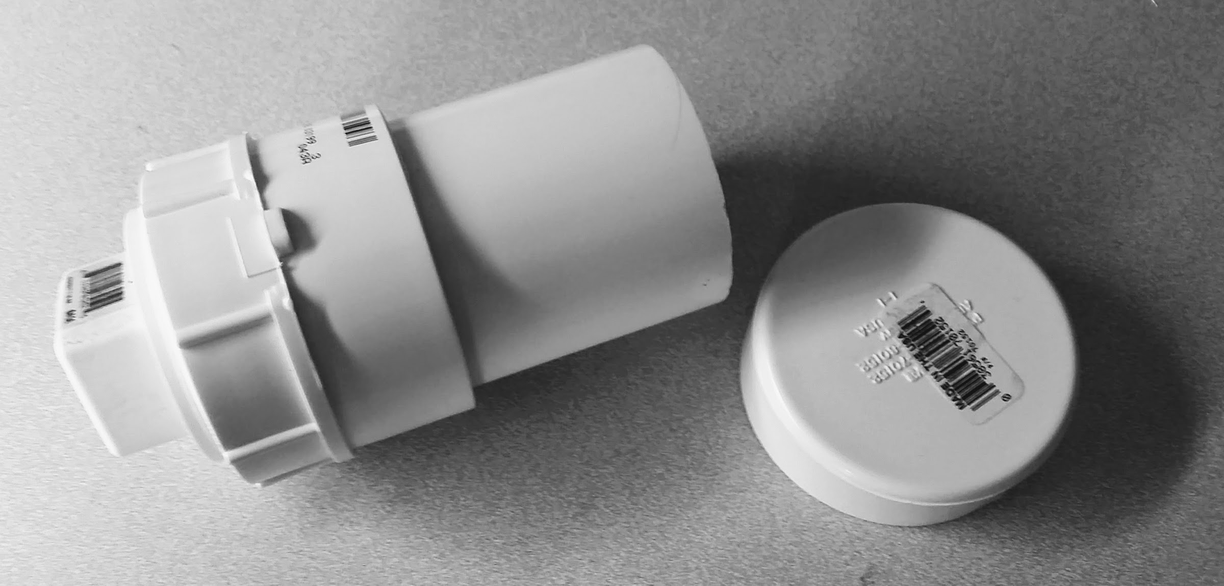
We are envisioning our enclosure design to be based on 2” PVC. It is easily obtained, easy to assemble, easy to machine/manipulate, and easy to make waterproof. In a perfect world, we’d design against 1.5” or 1” PVC, but for our first show, we’ll start with something “large enough” to be sloppy in our electronic design, but still have sensors “small enough” to be manageable.
Electronic Design: Custom 328P-based
We would like to use COTS components. For example, it would be nice to use Adafruit Feathers, or Sparkfun Quiic components. However, none of these boards are designed for extreme low power consumption; they fundamentally assume a hobbyist who is exploring programming embedded systems. This is not a criticism of these products, but it is not clear that (unmodified) we can say “purchase the 328P Feather and stack it up with…” as a sensor solution. I have to look closely at the Feathers, and do some testing to see “how low they can go” before I claim we cannot use them, but my concern is there is more going on on the board
(Part of “verbalizing” this process is so someone might say “but, Matt, you’re wrong…”)
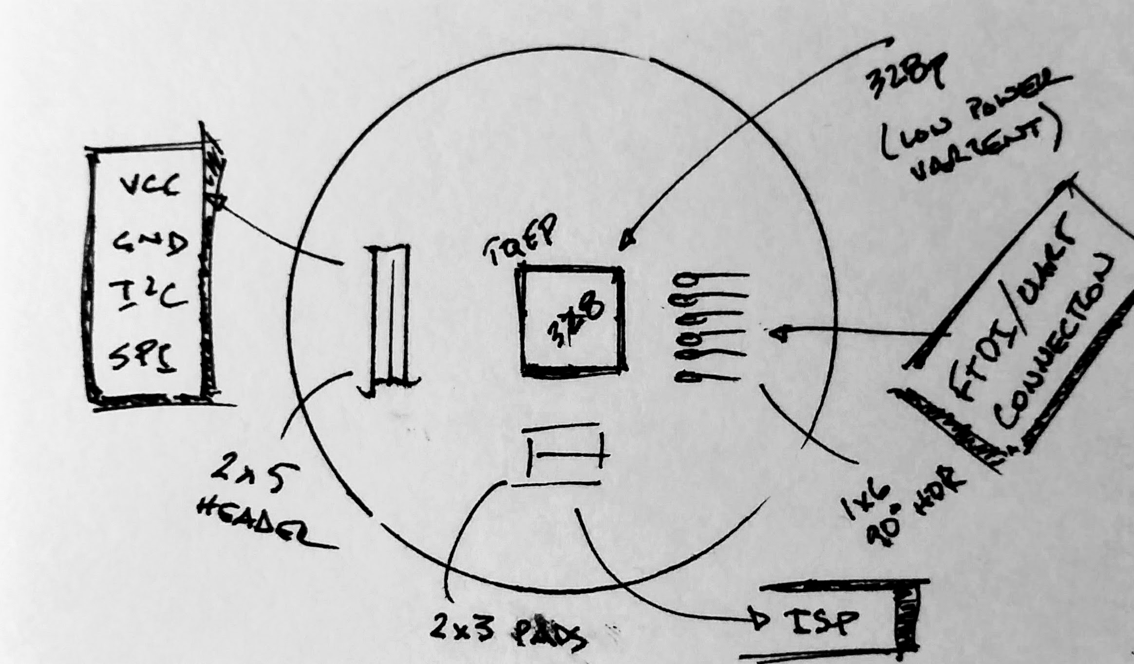
The idea is to have a stackable set of boards that are just under the 2” inside diameter of PVC. (This drawing is based on the OD, which is something like 2.375”, but it’s close.) I’m proposing the following:
A Main Board
- CPU. The main board has a 328P. The 328P will run at 3.3V/8MHz, reducing part count and power consumption.
- Bus Header. A 2x5 pin header will provide stackability, and through that header we will run VBATT, VREG, GND, I2C, and TWI/SPI.
- ISP. A six-pad (pogo-compatible) connection for the AVR ISP.
- USB-Serial. A six-pin (90˚ male) header for USB to serial.
- Status. A status LED.
This would be the “command” layer in a sensor stack. It has no functionality other than to have a CPU. For configurability, every other wafer in the stack has a single function as well, and stacks via the bus header. The rationale is that every single board will either have 1) an I2C-based device, 2) a SPI-based device, or 3) another 328P configured as an I2C listener device. (I’m going to reject the language of “master” and “slave”, and instead use “speaker” and “listener.”)
Note: The header might rather be breadboard compatible, instead of a 2x5? For example, a 1x5 row on the “top” and “bottom” of the board? Each side would want… VBATT, VREG, GND… and then control lines. On one side, SPI, on the other, I2C? Or, duplicate everything on both sides?
A Clock Board
- Clock. A DS3231M. This has a lower part count than the non-M variant; specifically, it does not require a crystal.
- Backup Battery. A CR2032 Battery.
Because the 3231 is already an I2C device, we know that, when plugged in, we can tell it to go into its deep sleep mode from the main board.
It can run off the VREG line in the bus header.
Note: This raises a question… should every board be populated so that it might have a regulator? Should that be something that is a “given” in the board design for a wafer, but we don’t choose until we actually populate a board and are laying out a sensing problem? For example, you might discover you must but the clock on VBATT with a regulator, because you simply have too much going on in your sensor stack to run everything off a single regulator. Or, perhaps (if there are two stacks, for breadboard compat.) we put two regulators on the distribution board, and the user can choose, with a jumper, whether one or both are active. That way, power from one side and power from another… No. There’s no easy way to choose which VREG you get your power from. Each wafter will be designed and implemented, and we don’t want to have jumpers everywhere…
Note: How does the DS3231 wake the controller? We might have to pass a “clock wakeup” GPIO line through the header?
An Analog Sensor Board
- Sensor Connectors. Three-Pin Connector(s)
- Listener Config. Address jumpers
- Listener. ATMega 328P
- ISP. ISP pads
- Power. Voltage regulator
Because we want to be able to turn off any analog sensors connected to the stack, we drop a 328 onto this layer. It is configured to listen to the command layer, so that a sensor developer simply plugs in this layer, can issue a “AnalogSensors.wakeUp(),” do a reading via “AnalogSensors.read(1),” and then tell the sensors to go back to sleep (“AnalogSensors.goToSleep()”). The 328P can source up to 40mA of current per pin, which for our sensors is more than enough (we’re in the 10-20mA range per sensor), so we should be able to source the current for the sensor directly from the processor.
Although code must be developed for this layer, it is primarily implementing an I2C “API” that the command layer will use. Once stabilized, we should never have to modify the analog sensor layer’s firmware, and instead can safely flash it to the board and leave it for the rest of time. If we need configurability (eg. wakeup time on a sensor, etc.), then we can expand, over time, the complexity of the firmware so we have defaults as well as reconfigurability built into the API.
Any sensing application that does not need analog sensors can, then, omit this layer of the stack.
This layer has a voltage regulator that can be optionally chosen via (solder) jumper. This may need to be a common option on many boards; a given stack may be able to run off a single regulator, or we many need multiple regulators in the stack, because peak current for the entire stack might exceeed what a single regulator can provide. (I’m thinking about possible high-current radio situations, for example.)
A uSD Storage Board
- Listener. ATMega 328P
- Listener Config. Address jumpers
- Storage. uSD slot
- Power. Voltage Regulator
The SparkFun OpenLog is a nice device, but pricy. Also, it stores data over serial; we need an I2C-based device to fit our stack. Ideally, we modify the OpenLog firmware, so that we can have a storage layer where we can wake up, store some data, and put the whole layer to sleep. Because the 328P is power miserly in deep sleep, we can use it (again) as an “API interface” for a common storage protocol for all storage layers.
By placing a 328P on this layer, we eliminate a great deal of code from the command layer. The command layer says “Storage.storeNext([array…])” or similar, and the driver handles squirting everything over I2C to the storage layer. If we develop the API reasonably, then the command layer can be ignorant of whether we are storing to a uSD or to a flash chip or FRAM. In short, we should be able to store sequential sensor readings easily, without worrying the developer about the particular medium they are storing to.
These abstractions will, ultimately, be limiting. But, they will be flexible abstractions. We can always improve the API running on the storage layers. For example, should a developer be able to issue a single command to “Storage.storeNextWithTimestamp([array…])”, or should the programmer be responsible for first getting a timestamp, combining it into a structure for storage, and then sending that to the storage layer? While not yet designed/decided, it is nice to know that these abstractions can be built, and the ultimate goal (of being able to quickly, reliably, program low-power environmental sensors) can be achieved.
Note: The voltage regulator should be one that has an ENABLE line. This way, the 328P can be used to enable/disable power to the uSD card.
A Radio Board
- Listener. ATMega 328P
- Listener Config. Address jumpers
- Radio. An ESP8266.
- Power. Voltage Regulator
We can go one of two ways on this board: it can have a listener and an ESP8266, or it can have just an ESP8266. The ESP8266 will drop into a reasonably low-power mode, but it is not as miserly as the 328P. As a result, we may want the intermediary, where the “wakeUp()” command will first wake the 328P, and it will then power up the ESP826.
In terms of software design, we would implement the same API (perhaps) on the 328P as a storage device. That way, storing data and sending data look exactly the same. The “smarts” for handling retry/etc. live on the local listener. The 328P, therefore, looks like every other listener: an I2C protocol implementation, and communication with the ESP8266 can be carried out over serial. This then looks like any Arduino sketch that uses an ESP8266 board, and allows us to use a stock firmware on the radio, as opposed to writing a custom controller in Lua or Python on the 8266. (If we later want to redesign this board, we can… but, it might be easier to start this way.)
If we must, we can use an ESP8266-01 module (with the six-pin header), or we can use a 12-E/F (and surface mount it). In other words, we could design this layer incrementally… one where we can prototype with a component we can plug in, and then evolve the design to one that we solder directly onto the board. There may be some question of using an external antenna… which would need to be inside the enclosure, but it could be done regardless.
I am worried about WiFi through the PVC in the field, but again… that’s what testing is for. This could become a LoRa radio, using a Nordic part. However, by using WiFi, we can have a base station that provides WiFi to cellular bridging as a COTS purchase. So… we’re really in a position where we want WiFi to “just work.”
Note: When we want to send data, how do we do it? Does the radio retreive everything since last send? Does the storage layer have “get everything since last transmission” API call? Or, does the controller have to shuffle everything from the storage, to the radio, and keep track of these things? In short, how smart is the stack? It would be nice to be able to say “Radio.transmitNewData()”, and it would handle talking to the storage layer (we would hand it an I2C address at setup), get the data, and send it. This suggests the storage layer has “Storage.getNewData()”, and it knows which datapoints are considered “new,” because it maintains an internal pointer that is updated everytime this is invoked. (We should also be able to “getNewDataPointer()” and similar.) Ideally, though, we can either squirt data directly at the radio from the controller, or the controller can hand off the issues of getting all of the data and sending it, so that the control code looks simple, and the complexity is implemented (once, and correctly) in the interface to all Radio and Storage layers.
Other Boards
Using the above board as examples, we also imagine boards that might have flash or FRAM for storage, boards where we connect I2C-based sensors, a power distribution board (where we have a voltage regulator and battery connections), and… so far, that might be it.
Benefits
For this project, it allows students to cut their teeth on circuit design one wafer at a time. Instead of trying to design a single board with everything on it, we design multiple boards that each do just one thing. This makes gives students the opportunity to design or revise wafers in (conceptual) isolation, as well as provide an ongoing source of projects. If we decide to scale down to 1.5” or 1” PVC, then we have a whole redesign process… but, can do it piecewise.
The stackable/wafer approach is also nice from a programming perspective; any board that has a local listener will be written to receive I2C messages, and do things in response. This makes the state machines for each wafer simpler to write: sleep, wake, process message, go back to sleep.
The individual wafers have no intelligence in the context of the overall sensor, which means we can develop and test each wafer’s API, have confidence in that wafer, and then integrate it into the sandwich stack. “Unit testing” of individual wafers is a huge win for this kind of application.
The controller is also interacting over a common protocol, and we can create small OO wrappers, so that we have a common API across all objects. Every board, for example, should have a “goToSleep()” method. We then develop the driver code so that where there are differences, we simply don’t care. That is, we call “Clock.goToSleep()” to put the DS3231 to sleep, even if that is actually a different set of I2C commands than if we put a storage layer to sleep; in either case, we invoke the “goToSleep()” method.
It is also designed for the enclosure. This is a problem with many COTS boards: they are designed as hobbyist boards that are breadboardable, but they are not designed for low power/extended battery usage, and they are not designed for a particular enclosure system. Here, we settle on PVC, and design against the constraints of a cylindrical enclosure.
We can reuse code from similar projects (Rocketscream’s low-power library, the OpenLog firmware may serve as a starting point for our storage layer), and we stay in the Arduino ecosystem with the lowest-power chip in that ecosystem.
Related Systems
It would be nice to be able to buy Adafruit Feathers, design against the Feather “standard,” and be done. However, Feathers are not designed for low power usage. So, we could pick the standard, but we would be in a position of designing all new boards.
That said… Feathers are open source. Therefore, we could take (say) the 328P board, rip off anything we don’t want, and then use it.
But, we would need to 3D print a harness that held the Feathers at an angle to fit in the board, or run them along the central axis… and, then, we would have limited-or-no stackability. This eliminates the benefits of the Feather as a formfactor.
Quiic (from Sparkfun) has no way to control power on each board. There’s no form-factor standard. There’s no clear way to mount them in a given enclosure. If we use PVC, we will end up with a mess of boards wired to each-other, which feels… messy. It lacks support for SPI, which may (for some sensors) be critical to our applications. There is no provision for GPIO signaling if we absolutely need it.
Grove has similar drawbacks to Quiic, but lacks the commitment to a single protocol.
Drawbacks
We have to design everything.
We have to develop the API, and write all of the code.
We aren’t starting with a CircuitPython-compatible CPU. It would be really nice to design with the SAMD21 or SAMD51, but… with limited experience, and unknown library support, this could lead us into a space where we’re doing more embedded software engineering with students new to embedded design than we like. We can always transition over time; because we are designing against an I2C API, we can (for example) replace the controller board with a CircuitPython-ready CPU, and program it in Python, and still have the same abstractions.